
Reverse engineering a PCB is a five-step process: intake and documentation, layer-by-layer imaging and netlist extraction, schematic reconstruction, BOM cross-reference, and verification. Skipping any step turns a recoverable board into a costly failure downstream.
What PCB reverse engineering actually means
PCB reverse engineering is the reconstruction of a circuit board's design data — schematic, connectivity, component list and manufacturing files — from the physical board itself. It's used when original documentation is lost, when a board must be rebuilt after component obsolescence, or when a working design needs to be understood before it can be repaired, improved or manufactured again.
The craft is not in reading copper; modern imaging does that. The craft is in verification — proving that what was reconstructed is what the board truly is, net by net. That discipline separates a rebuild that works from a rebuild that looks right. Here's how the full process runs on our benches (the service itself is described on the reverse engineering page):
| Step | What happens | What skipping it costs |
|---|---|---|
| 1. Intake & documentation | Board photographed, X-rayed, condition mapped | Damage and unknowns get "read" as design intent |
| 2. Layer imaging & netlist extraction | Copper recorded layer by layer, connectivity extracted | Invisible inner-layer errors baked into the rebuild |
| 3. Schematic reconstruction | Netlist becomes a verified, reviewable schematic | A netlist nobody can sanity-check — errors hide in plain sight |
| 4. BOM identification & cross-reference | Every part identified, classified and cross-referenced | Wrong or unbuyable parts specified for the rebuild |
| 5. Verification build & test | Reconstructed design is fabricated, assembled, tested | "Looks right" boards that fail at power-on |
STEP 01Intake, documentation and non-destructive analysis
Before anything is taken apart, the board is documented exactly as it arrived: high-resolution photography of both sides, X-ray imaging where internal structure matters, and a condition map that marks burnt regions, previous repairs, corroded traces and anything else that makes this board different from a clean original.
Everything the customer still has joins the record — partial schematics, old BOMs, firmware images, test procedures. Even outdated fragments shrink the problem space dramatically.
This is also where the project's legal footing is confirmed: reverse engineering is routine when you own the board or the design rights, but the ownership question should be settled before the teardown, not after.
A charred area or a bodge wire from an old field repair looks exactly like design intent if you don't know it's there. Undocumented damage is the number-one source of "mystery behavior" in rebuilt boards.
STEP 02Layer-by-layer imaging and netlist extraction
The board is then carefully depopulated and its copper recorded layer by layer — external layers through high-resolution scanning, internal layers through progressive removal and imaging, with X-ray support for hidden routing and cross-sectioning where fine geometry demands it.
The images are registered to each other and the geometry is converted into raw connectivity: every pad, trace, via and plane segment becomes graph data. From this, the true netlist — the board's actual electrical connectivity — is extracted.
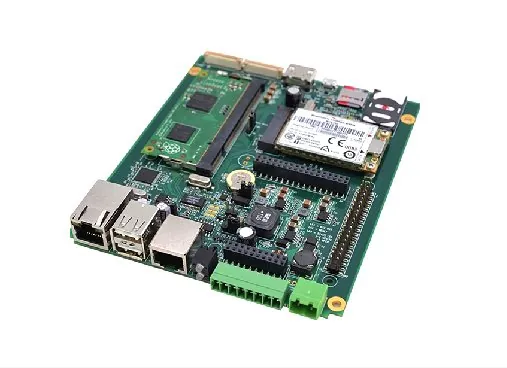
Inner-layer errors are invisible on the assembled board. A single misread buried via passes every visual check — and shorts two nets the moment the rebuild is powered.
STEP 03Schematic reconstruction and review
Raw connectivity is not yet a design. In this step the netlist is organized into a human-reviewable schematic: components placed into functional blocks, power distribution traced, signal chains drawn in logical order. Someone who understands the circuit can now read it — and question it.
That review is the point. A schematic is a hypothesis about the board; engineering review tests it. Does this regulator topology make sense? Why are there two clock sources? Is that test point network for production programming? Every question resolved here is a defect prevented downstream.
An unreconstructed netlist can't be sanity-checked by a human. Topology errors that any engineer would catch in a schematic sail through raw connectivity data undetected.
STEP 04BOM identification, cross-reference and lifecycle audit
Every component is identified — by marking where legible, by package and circuit context where not — and the BOM is built line by line. Then each line is classified: active, not recommended for new designs, or end-of-life. Discontinued parts get current cross-references with comparable specifications.
This is where a rebuild becomes sustainable. A board re-created with EOL parts is a museum piece; the same board re-created with orderable parts is a product. (We cover this in depth in beating component obsolescence.)
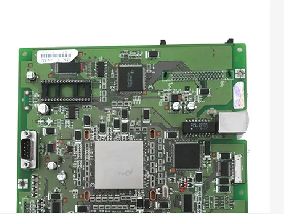
A "probably equivalent" substitution that differs in gate threshold, timing or startup behavior will pass assembly and fail in the field. Component substitution is engineering, not purchasing.
STEP 05Verification: prototype, compare and test
The reconstructed design is manufactured — new Gerbers fabricated, the board assembled with the audited BOM — and the result is tested against the original. Electrical test verifies the netlist. Inspection confirms workmanship. Functional test checks the behaviors that mattered on the original board, ideally in the actual equipment it came from.
We treat verification as its own engineering discipline, not a formality — the layered test strategy is described in why rigorous PCB testing is crucial after reverse engineering, and the capability lives with our PCBA testing team.
This is the only step that catches reconstruction errors after the fact. Skipping it doesn't remove the errors — it ships them.
What you receive when it's done
A completed reverse engineering project hands you the same data a forward-designed project would have:
- Reconstructed schematic — verified, reviewable, editable for future revisions
- Verified BOM — every part identified, lifecycle status flagged, alternates cross-referenced
- Manufacturing-ready Gerbers — fabrication data generated for modern processes
- Redesign recommendations — DFM notes and modernization options for manufacturability
With those deliverables, the board stops being a stranded asset and becomes a design you can build, revise and support — like any product you own. And when the same team that recovered the design also fabricates, assembles and tests it, the verification loop closes inside one roof — a point we make in why splitting RE from manufacturing costs time and money.